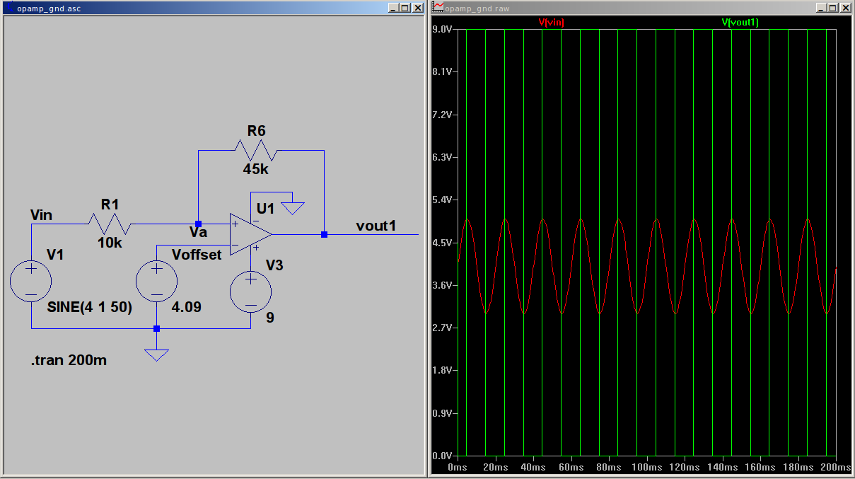
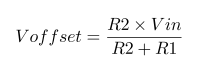
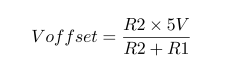
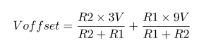
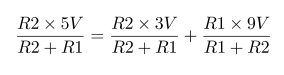
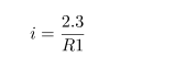
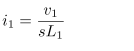
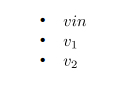
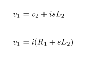
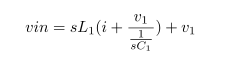
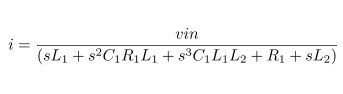
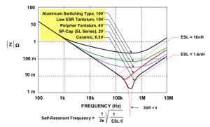
Impedance of Various 100μF Capacitors :
-
The figure tells us that the impedance of a capacitor will decrease monotonically as frequency is increased.
-
In actual practice, the ESR causes the impedance plot to flatten out.
-
As we continue up in frequency, the impedance will start to rise due to the ESL of the capacitor.
-
The location and width of the “knee” will vary with capacitor construction, dielectric and value.
-
This is why we often see larger value capacitors paralleled with smaller values. The smaller value capacitor will typically have lower ESL and continue to “look” like a capacitor higher in frequency.
-
This extends the overall performance of the parallel combination over a wider frequency range.
Reference : From Analog Devices Tutorial
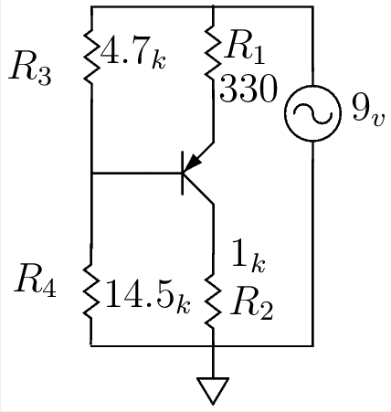
Frequency Characteristics of a 0.1 uf Capacitor :
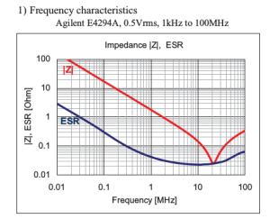
The impedance matches with ESR at around at around 2 Mhz.
ESL Analysis :
Frequency = 20 Mhz
Capacitance = 0.1 uF
From the frequency equation , ESL = 0.63 nH
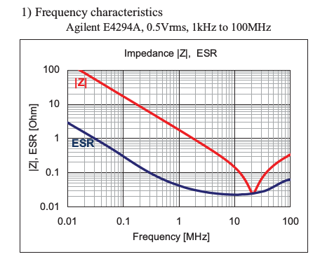
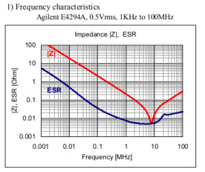
Frequency Characteristics of a 1 uf Capacitor :
The impedance matches with ESR at around at around 8 Mhz.
ESL Analysis :
The impedance matches with ESR at around at around 8 Mhz.
Frequency = 8 Mhz
Capacitance = 1 uF
From the frequency equation , ESL = 0.39 nH
The impedance matches with ESR at around at around 2 Mhz.
ESL Analysis :
Frequency = 2 Mhz
Capacitance = 10 uF
From the frequency equation , ESL = 0.63 nH
Frequency Characteristics of a 10uf Capacitor :
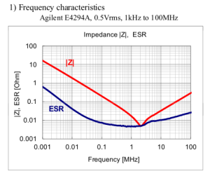
The impedance matches with ESR at around at around 2 Mhz.
ESL Analysis :
Frequency = 2 Mhz
Capacitance = 10 uF
From the frequency equation , ESL = 0.63 nH
Capacitor Graph Reference : Datasheets from Digikey